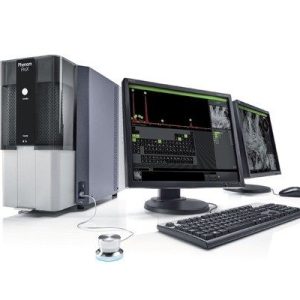
Scanning electron microscope (SEM) with EDS
Scanning electron microscope (SEM) with EDS
 avec EDS")
| MANUFACTURER | FEI |
|---|---|
| MODEL | Inspect F50 |
General description:
Scanning electron microscopy (SEM) is a powerful imaging technique to study the morphology (shape, size, particle arrangement, etc.), surface topology (relief, texture, etc.), and chemical composition (relative ratios of chemical elements from carbon to uranium) of a sample. The SEM uses a focused beam of high-energy electrons to generate a variety of signals at the surface of solid specimens revealing information about the sample.
Applications:
SEM is used to analyze a multitude of samples of all shapes, compositions and sizes for samples stable under high-vacuum conditions.
Characteristics :
SEM is a non-destructive analytical method for electrically conductive material. The study of insulating materials, on the other hand, requires extra step for sample preparation including the deposition of thin conductive layer (carbon or palladium alloy).
- Practical magnifications ranging from 10X to 300,000X.
- Secondary electron (SE), backscattered electron (BSE), or X-ray mapping images.
- Spectrometer for energy-dispersive X-ray analysis (EDAX).
- Digital imaging.
To use this equipment
The equipment available is accessible to the academic and industrial research community.
To learn about usage conditions and availability, please fill out the form below. After reviewing your request, we will contact you shortly to offer you the best available solution.