+PRECISE +SMALL +EFFICIENT
Since the invention of the first microprocessor in 1971, the relentless reduction of the limits of device fabrication, from 3 microns in 1980 to 32 nanometres today, has given rise to a constant evolution of microelectronics, which should continue until it reaches a fast-approaching physical “wall”: the atom. In fact, 32 nanometres represent only one hundred or so atoms placed side by side: the challenge lies in producing structures with a resolution of only a few atoms over large surfaces, and at a lower cost.
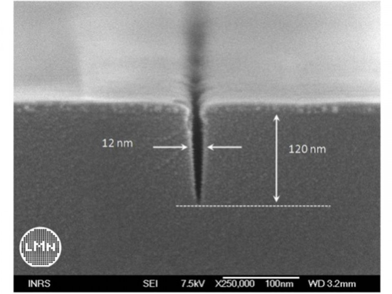
The production of structures this size is based on two major steps: the definition of motifs in resist and their transfer to the material. To push back the limits of these steps, the Vistec VB6 UHR-EWF — one of the world’s most efficient electronic lithography tools — is put to effective use. Couples to plasma etching tools at the cutting edge of technology, motifs approximately 10 nm wide (i.e. about thirty atoms) etched to a depth of 120 nm were produced on Si and SiO2, the smallest sizes ever achieved.
RESEARCHERS
S. Delprat, B. Le Drogoff and Prof. M. Chaker (INRS)
