
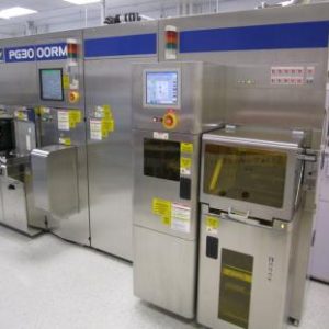
Wafer inspection (scanner)
Wafer inspection (scanner)
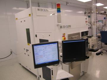
| MANUFACTURER | Rudolph Technologies, Inc. |
|---|---|
| MODEL | WS3880 |
General description:
Automated wafer inspection prior to dicing
Characteristics :
- Automatic slice support:
- 200 and 300mm
- Thickness from 800µm to 190µm
- Maximum number of bump / slice: 10 million
- 2D optical detection: 5µm
- 3D laser detection: 0.125µm, 4 MHz data acquisition rate
- Depth of field: 28µm (2D), 200µm (3D)
- Very high resolution 3D detector: 5µm
- 5-position lens turret: 1.25X, 2X, 5X, 10X)
- Bright and dark field lighting
- 2D metrology and bump fault detection
- 3D measurement of height and coplanarity of bumps
- Electronic slice mapping
- Integrated ISO class 2 filtration unit
- Remote computer fault review
To use this equipment
The equipment available is accessible to the academic and industrial research community.
To learn about usage conditions and availability, please fill out the form below. After reviewing your request, we will contact you shortly to offer you the best available solution.