
Chip placement Panasonic
Chip placement Panasonic
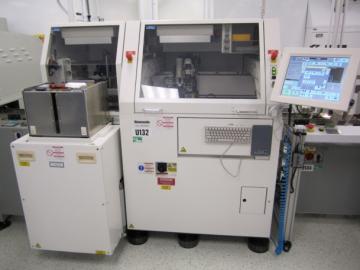
| MANUFACTURER | Panasonic |
|---|---|
| MODEL | FCB3 |
General description:
Automated high precision multi-chip die bonder for positioning and attaching small electronic components on printed circuit board or substrate
Characteristics :
- JEDEC tray input/output
- Accuracy +/- 3 µm @ 3 sigma cpk 1.33
- Automatic calibration function to correct thermal changes over time
- Simultaneous recognition camera with temperature control
- Chip to substrate and chip to wafer capable
- Placement head for flip chip
- Thermo compression head available
- Bonding pressure 5N – 490N
- 4 points parallelism adjustment system
- Bonding head temperature up to 500˚ C
- Heated bonding stage JEDEC format up to 250˚C
- Ceramic heated bonding stage for 300 mm wafer up to 200˚C
- Multi-chip placement in one single pass capability
- Flux dipping station
- Die pick from wafer (up to 12 inches), waffle pack or GEL-PACK ( 2 x 2 inches)
- Wafer table with stretcher
- 2 positions automatic tool changer unit
- SECs/GEM capability
- Wafer scanner and electronic wafer mapping capable
- Pattern recognition system with edge, gray level, pattern and ink dot
- Wafer size 150/200/300 mm on 300 mm wafer frame
- Max quantity/wafer x=200 chips, y=200 chips
- Frame size 375 mm
- Die size 1 mm to 35 mm
- Die thickness 0.05 to 7 mm
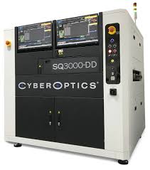
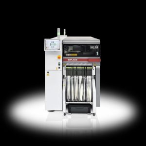
To use this equipment
The equipment available is accessible to the academic and industrial research community.
To learn about usage conditions and availability, please fill out the form below. After reviewing your request, we will contact you shortly to offer you the best available solution.