
Electrodeposition of metal and dielectric
Electrodeposition of metal and dielectric
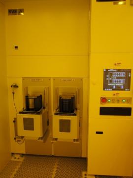
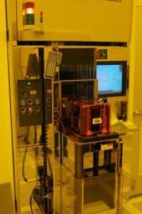
| MANUFACTURER | Scientific Value Solutions Corp. (SVS) |
|---|---|
| MODEL | JikJi-77 |
General description:
Through Silicon Via filling of copper and Au-Sn
Characteristics :
- Wafer size: 200 mm
- Thickness range of wafers: 300 – 1200 µm
- Wafer material: Silicon, Glass
- Fully qualified for through silicon via AquiViaTM process under license from Alchimer, with the following modules:
- Module 1: Pre-wetting of Si wafers with 20:1 aspect ratio vias
- Module 2: Chemical grafting of 0.2-1.0 µm insulation film
- Module 3: Activation of insulation for Ni(B)
- Module 4: Electroless Ni(B) diffusion barrier
- Module 5: Cu electrofill in 50:5µm & 100:5µm TSV
- Module 6: Wafer annealing
- Module 7: 80Au/20Sn eutectic electroplating
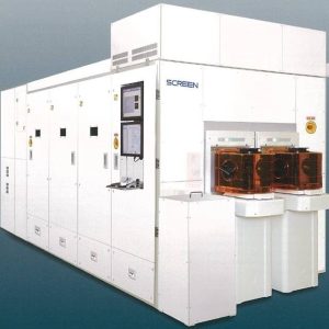
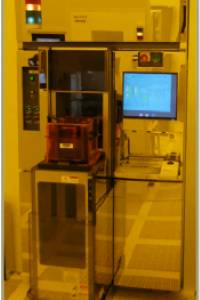
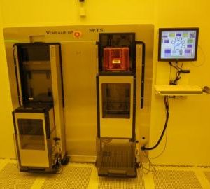
To use this equipment
The equipment available is accessible to the academic and industrial research community.
To learn about usage conditions and availability, please fill out the form below. After reviewing your request, we will contact you shortly to offer you the best available solution.