
Polishing and planarisation
Polishing and planarisation
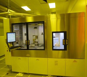
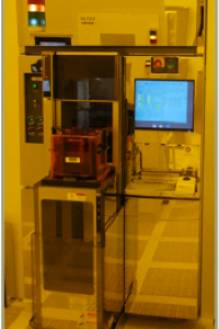
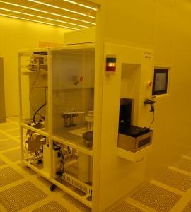
| MANUFACTURER | Strasbaugh |
|---|---|
| MODEL | STB P300/ 6EH |
General description:
Polishing silicon, silicon dioxide, copper and tungsten on 200 mm wafers
Characteristics :
- Automated wafer handling
- Compatible cleaning modules for copper/tungsten through-silicon-via processes
- Standard silicon and polysilicon polishing
- Standard silicon oxide polishing and planarization
- Standard copper planarization
- Standard tungsten planarization
- Thickness range of wafers: 300 – 1200 µm
- Post-CMP wafer-to-wafer thickness non-uniformity: 9% (3 sigma)
- Post-CMP polishing within wafer thickness non-uniformity: 15% (3 sigma)
- In-situ metrology with end-point detection
- Dry-in, dry-out with in-situ clean operation
- Double-side scrub, megasonic clean
- Bulk delivery of slurries and chemicals
To use this equipment
The equipment available is accessible to the academic and industrial research community.
To learn about usage conditions and availability, please fill out the form below. After reviewing your request, we will contact you shortly to offer you the best available solution.