
Chip placement Finetech
Chip placement Finetech
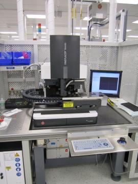
| MANUFACTURER | Finetech |
|---|---|
| MODEL | Fineplacer Femto Die Bonder |
General description:
Fully automated bonder for positioning and attaching small electronic or opto-electronic components on printed circuit board or substrate.
Characteristics :
- Ideal for product and process development
- Placement, thermo compression bonding capable
- Forming gas and formic acid available
- Automated pattern recognition, alignment and bonding
- Overlay vision alignment system with fixed beam splitter in combination with automatic field extension and zoom
- Live process observation camera
- Placement accuracy: 0.5 µm
- Field of view: 0.27 mm x 0.2 mm (min) 3.2 mm x 2.4 mm (max)
- Component size: 0.125 mm x 0.125 mm (min) 80 mm x 80 mm (max)
- Working area: 450 mm x 150 mm (max)
- Z travel / resolution: 10 mm / 0.2 µm
- Y travel / resolution: 150 mm / 0.1 µm
- X travel / resolution: 450 mm / 0.1 µm
- Theta travel +/- 9˚ / resolution; 0.2 m˚
- Bonding force max : 500 N
- Heating temperature max : 450 ˚C
To use this equipment
The equipment available is accessible to the academic and industrial research community.
To learn about usage conditions and availability, please fill out the form below. After reviewing your request, we will contact you shortly to offer you the best available solution.