
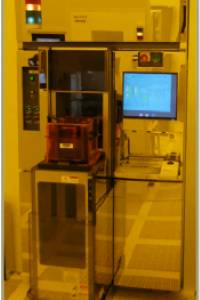
Plasma enhanced chemical vapour deposition
Plasma enhanced chemical vapour deposition
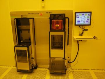
| MANUFACTURER | SPTS |
|---|---|
| MODEL | Versalis FxP APM200 |
General description:
Plasma-enhanced Chemical Vapour Deposition of amorphous Silicon, Silicon Nitride, Tetraethylorthosilicate (TEOS)
Characteristics :
- Wafer size: 200 mm
- Thickness range of wafers: 300 – 1200 µm
- Temperature range: 100 – 400 °C
- Pressure range: 0.1 – 10 Torr
- Gases used: O2, N2, SiH4, NH3, He, Ar, TEOS, C3F8
- Wafer material: Silicon, Glass, Bonded wafers
- Processes:
- 0.5 -1 µm thick film of Silicon Nitride deposited at 300 °C
- 1 – 2.5 µm thick film of TEOS deposited at 300 °C
- 0.5 -1 µm thick film amorphous Silicon deposited at 300 °C
To use this equipment
The equipment available is accessible to the academic and industrial research community.
To learn about usage conditions and availability, please fill out the form below. After reviewing your request, we will contact you shortly to offer you the best available solution.