
Wafer bonding
Wafer bonding
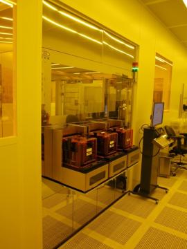
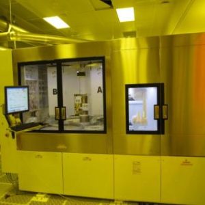
| MANUFACTURER | EV Group |
|---|---|
| MODEL | GEMINI/200/3 |
General description:
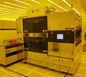
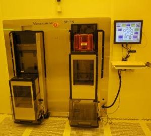
Fully-automated wafer bonding for 200 mm wafers
Characteristics :
- Processing 200 mm wafers and 3D-Integrated MEMS devices with wafer-level packages.
- Bond 200 mm wafers using fusion bonding, glass frit bonding, adhesive bonding, eutectic bonding, thermo-compression bonding, transient liquid phase bonding, and solder bonding.
- Wafer-to-wafer alignment accuracy: ± 0.4 µm (3 sigma)
- Range of wafer thickness: 300 – 1700 µm
- Temperature control: 20 – 550 °C ± 1.5%
- Contact Force control: 1.5 – 100 kN ± 2%
- Gas pressure control: 0.1 – 1000 mbar ± 5%
- In-situ wafer treatment with formic acid vapour
- Megasonic wafer cleaning

To use this equipment
The equipment available is accessible to the academic and industrial research community.
To learn about usage conditions and availability, please fill out the form below. After reviewing your request, we will contact you shortly to offer you the best available solution.