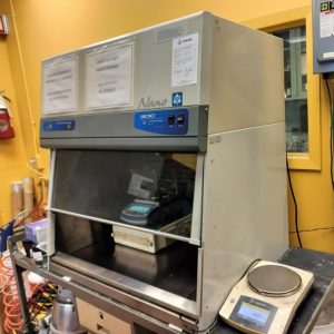
Magnetron Sputtering
Magnetron Sputtering
Additional information
| MANUFACTURER | N/A |
|---|---|
| MODEL | N/A |
Samples
- Sample size : 1 mm to 100 mm (4 in.)
- Wafer uniformity : 13% on 100 mm (4 in.
Characteristics
- Pressure : up to 1×10⁻⁶ Torr
- Pass through for sample transfer
- Target types : 50 mm (2 in.) diameter, 99.9% purity
- Substrate types allowed: semiconductors, metal and plastics
- Gas: Ar, N2, O2
- Deposition rate: 1 to 10 Å/s
ROUTINE PROCESS
Silicon Deposition
- Thickness: from 10 nm to 2000 nm
Metal Deposition
- Type: Au, Cr, Ni
- Thickness: from 10 nm to 2000 nm
ROUTINE PROCESS
Oxide Deposition
- Type: ITO, silicon dioxide
- Thickness: from 10 nm to 20000 nm
Nitride Deposition
- Type of nitride: silicon nitride
- Thickness: from 10 nm to 2000 nm
To use this equipment
The equipment available is accessible to the academic and industrial research community.
To learn about usage conditions and availability, please fill out the form below. After reviewing your request, we will contact you shortly to offer you the best available solution.

